
Wafer loader
Wafer Menari MPLS, Apakah itu? Ternyata ini Arti dan Jawaban Tebak-Tebakan atau Teka-teki MPLS MOS OSPEK 2023 (Pexels: Sylwester Ficek) 82. Hari kenyal = yupi. 83. Minuman genit = marimas. 84. Roti timur tengah = kebab. 85. Susu tengkorak = boneto. 86. Nasi hepatitis = nasi kuning. 87. Ciki bohong = lays.
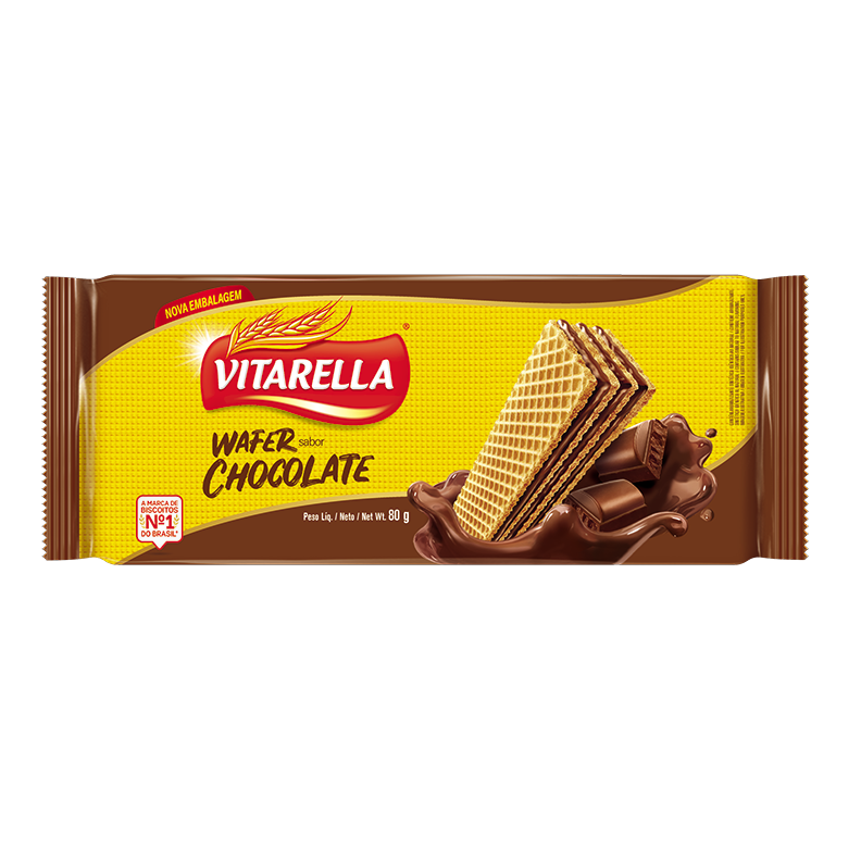
Wafer Chocolate Vitarella Tem diferença. Tem sabor.
Historical development of the wafer size. The manufacture of integrated circuits on silicon wafers started in the mid 1960s on wafers with a diameter of 25 mm. Nowadays, in modern semiconductor manufacturing wafers with a diameter of 150-300 mm are used. By 2012 the mass production of microchips on wafers with a diameter of 450 mm is expected.
Garuda Halal
Manufacturing: Making Wafers. To make a computer chip, it all starts with the Czochralski process. The first step of this process is to take extremely pure silicon and melt it in a crucible that.

Harga Richeese Nabati Wafer Wafer Murah Terbaru 2023
Apa itu wafer menari? merujuk pada istilah yang memiliki makna dan signifikansi tertentu. Untuk memperoleh pemahaman yang lebih mendalam mengenai istilah ini, silakan merujuk pada tabel di bawah ini. Tabel tersebut menyediakan penjelasan sederhana mengenai arti, makna, dan maksud dari wafer menari. Artinya disusun berdasarkan subjek.

Wafer Bar
Wafer bonding is a process for temporary or permanent joining of two or more wafers with or without an intermediate layer. Wafer bonding has various applications: packaging (e.g. for sensors and actuators), assembly (e.g. for RF components), integration (e.g. for electrical/micromechanical/optical component), substrate and device fabrication.The System Packaging department offers standard.
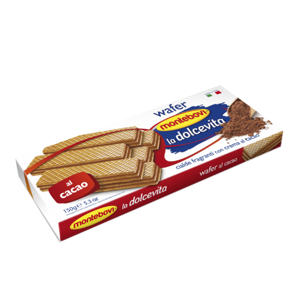
Wafer Montebovi
In this study, two methods are introduced for scalable and wafer-scale manufacturing of metalenses operating in the near-infrared region, aimed at overcoming the abovementioned challenges. The first type of metalens is polarization-independent and constructed using hydrogenated amorphous silicon cylindrical structures fabricated through direct.
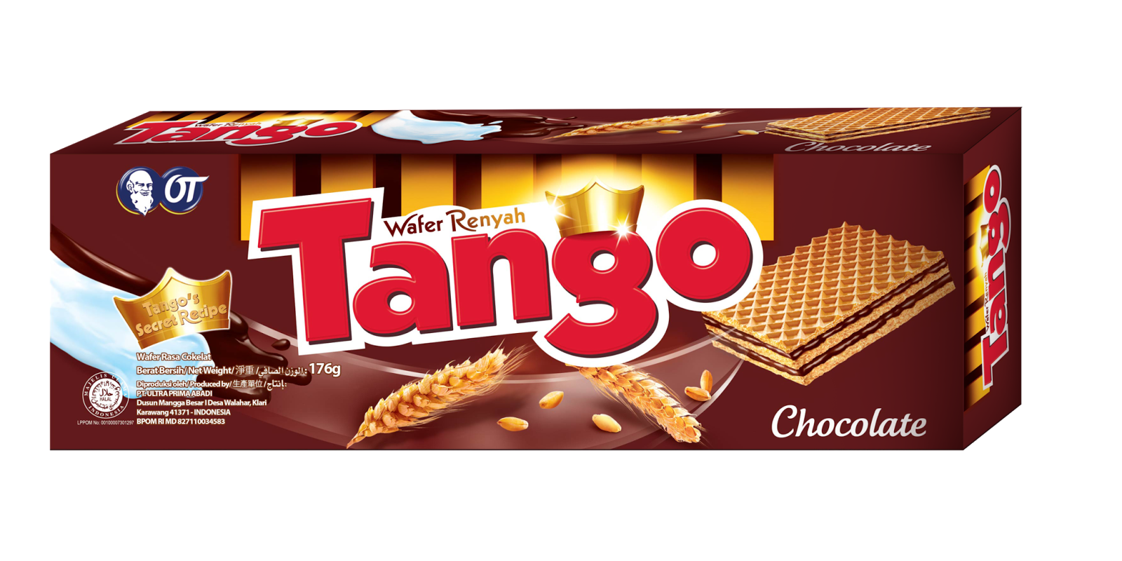
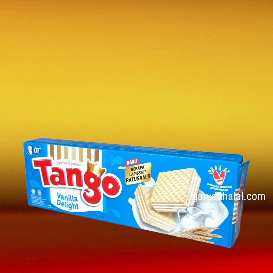
Harga Wafer Tango Di Alfamart Terbaru
In electronics, a wafer (also called a slice or substrate) is a thin slice of semiconductor, such as a crystalline silicon (c-Si), used for the fabrication of integrated circuits and, in photovoltaics, to manufacture solar cells.. The wafer serves as the substrate for microelectronic devices built in and upon the wafer. It undergoes many microfabrication processes, such as doping, ion.

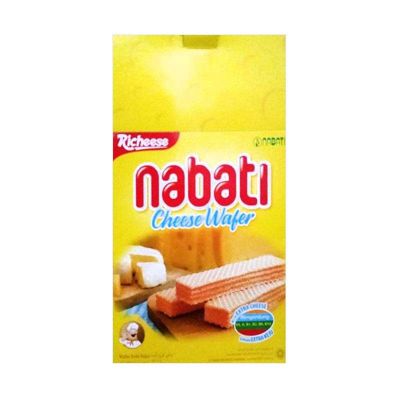
Jual Richeese Nabati Cheese Wafer [50 g] di Seller Coco Mart Official Store Jimbaran, Kab
A wafer is a thin, usually round slice of material that's shiny. It's important for making electronic chips. To make it, we go through four main steps: growing a crystal, turning it into a wafer, polishing the wafer, and getting it ready for use. First, we make a crystal with special properties.

Wafer Menari Artinya Adalah? Apa? Dalam MOS MPLS OSPEK
Wafer-sized multifunctional polyimine-based two-dimensional conjugated polymers with high mechanical stiffness. Nat. Commun. 7, 13461 doi: 10.1038/ncomms13461 (2016).
Jual Richeese Nabati Wafer [20 pcs] di Seller larees manees Cacaban, Kota Magelang Blibli
Here, the authors demonstrate the application of machine learning to optimize the device fabrication process for wafer-scale 2D semiconductors, and eventually fabricate digital, analog, and.
wafer,United Arab Emirates price supplier 21food
The SOI wafer had a pre-set pFET array (Fig. 7 a). By transferring the MoS 2 from the sapphire substrate to the SOI wafer (Fig. 7 b), a 3D stacking structure was formed, with the top MoS 2 used as the n-channel. The entire transfer process was carried out at low temperature to minimize the degradation of the bottom silicon device.

Napolitan wafers cocoa 60g IMPOL HOLDING
The Si wafer industry has extremely well defined SEMI specifications, and a general outline as to how to properly locate these specifications is given here. Specifications for thin wafers, Double Side Polished wafers, strange diameter wafers, 1" wafers, and other custom and semi-custom wafers are not strictly related to the SEMI M1-0302.
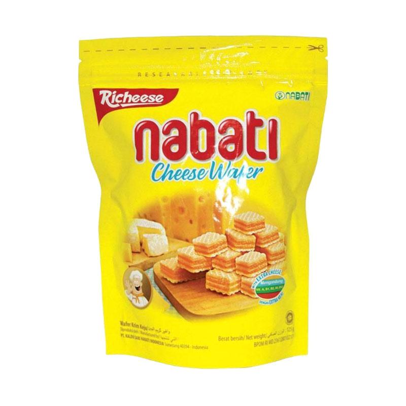
Jual RICHEESE Keju Wafer Nabati [125 g/ Pouch] di Seller Klikgo Panjer, Kota Denpasar Blibli
The process of manufacturing semiconductor wafers involves a series of complex stages. Firstly, a single crystal of semiconductor material is grown using a process called crystal growth. This entails heating the material to a high temperature and then gradually cooling it down. Secondly, the crystal is sliced into thin wafers using a diamond.
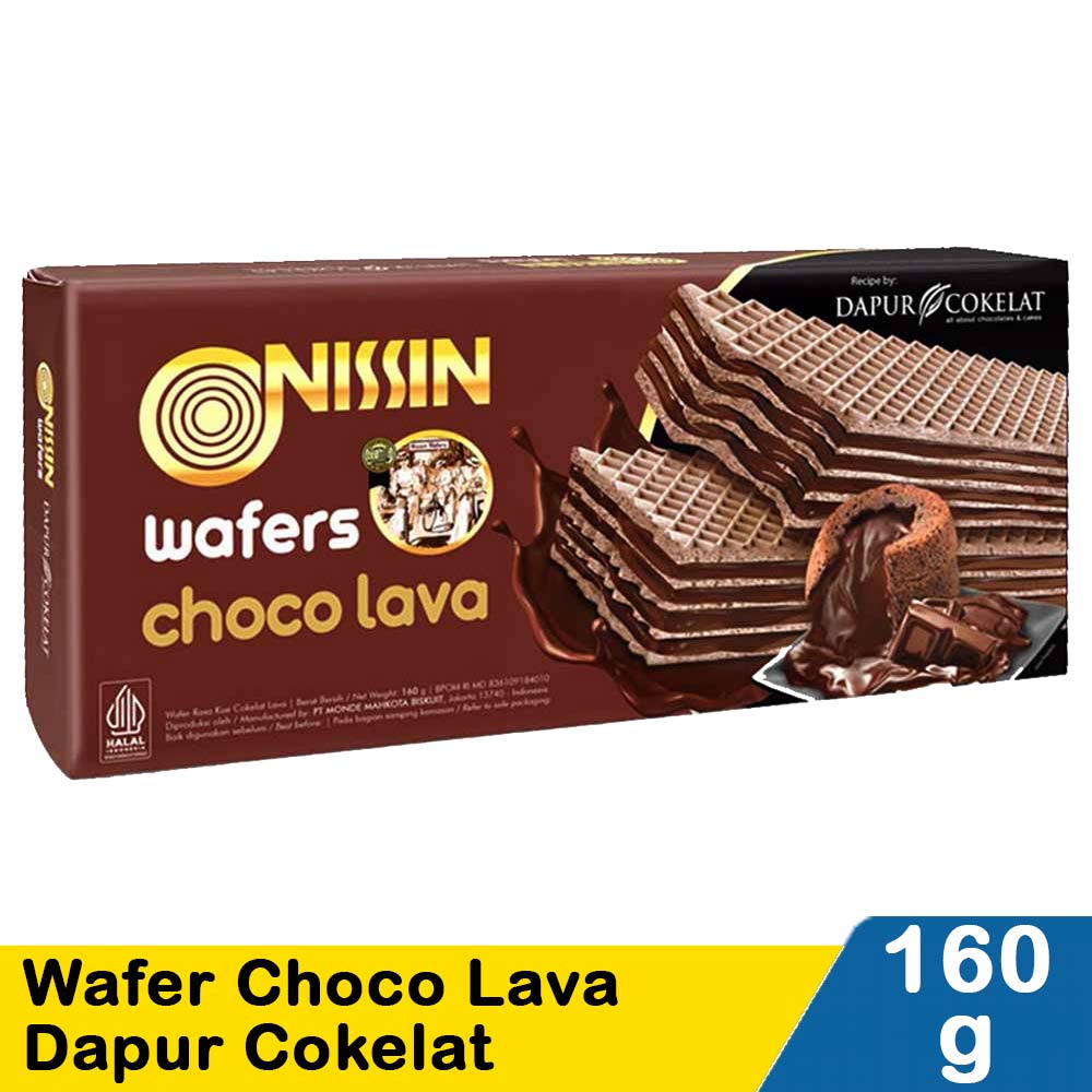
Nissin Wafer Cream Dapur Cokelat Choco Lava 160g Klik Indomaret
In this work we report the fabrication of ordered arrays of sub and micron-scale silicon pyramids and pillars by simple electrochemical etching of a p-type silicon substrate through Pd deposition. The Pd was deposited on Si substrate by evaporation technique using a mask (mPd/Si) and without a mask (wPd/Si). The morphology and dimensions of the silicon nano or micro-structure were controlled.

Wafer rolls
These wafers were small, expensive, and had limited applications. Early semiconductor devices were bulky and unreliable. Transition to Larger Wafers (1970s-1980s) With the advent of integrated circuits, there was a demand for larger wafers. Manufacturers started producing 2-inch wafers, eventually scaling up to 8-inch wafers.

JAWABAN Wafer Menari Tekateki MPLS 2023 Ternyata Adalah ini, Simak Arti dan Jawaban Tebak
Abstract. Wafer-to-wafer bonding techniques are widely used in the semiconductor industry to create a range of complex devices which are now used in many industrial, consumer, and automotive applications. In the following chapter, the main bonding techniques utilized in MEMS components are described and some study cases presented.
